

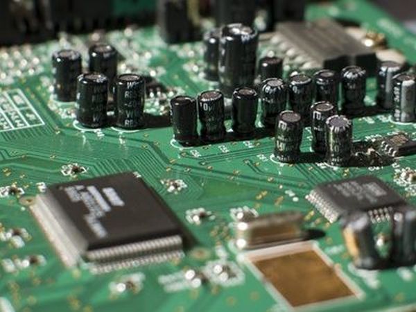
The market of electronics is changing at a rapid pace and if you observe it closely then you’ll find that innovation is one of the most vital features that one looks in an electronic product these days. Developing and making the electronics for the forthcoming generation is a tough job to handle as innovation and advancement is on its peak and the designers have to surpass these standards in order to succeed in the highly competitive world of today. Among the technological changes that are ongoing now-a-days innovation certainly rules and you cannot expect a good market for an electronic that is sans innovation.
The designers who understand the importance of an innovative design and incorporate the same in their creation take a step forward and the designers who fail to grasp the importance lag behind and are often out of the competition within no time. The customers today want electronics that are multi functional, slim in design, light in weight and compact in shape. Apart from all these features they also expect the device to be affordable. The process of designing an electronic is getting complex by the day and the traditional design equipments are being pushed beyond their limits.
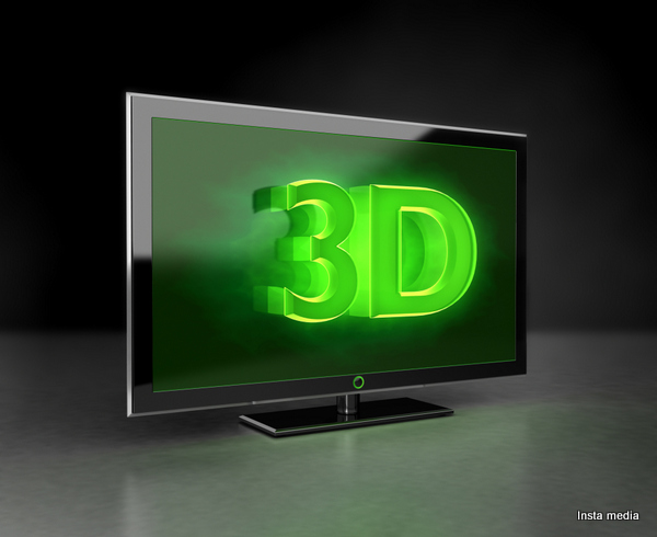
The PCB complexity does not end here as the growing number of nets and tougher design constraints only add to the complexity. It is a good thing to know that the PCB tools have evolved with the time and they are able to face the challenges that come their way. The 3D capabilities are considered as a vital change and it is also expected that they will bring on the revolution the in the manner the designers make their products. Let us discuss the same in more detail.
Designing innovative electronics in a world of 3D
Conventionally the people who design the circuit have highly relied on design models to confirm the function, fit as well as form before the fabrication but the main thing to note here is that this method has not one but many minus points. One of the major drawbacks is that PCB development has always been completed in 2D and then the process of making them 3D begins which is quite time consuming in nature. The designers are in urgent need of a design tool which is equipped with advanced 3D features.
This will allow the designers to preview the 3D images of their work before the fabrication process and thus getting rid of the mockups. The overall value of 3D ability is quite pivotal in PCB design and therefore today there are various firms that extend such services. In order to get the maximum benefits of the 3D equipments it is more than necessary for the designers to use PCB solution. The facility to make 3D animation or video can be very useful for the designers as that way they can easily share and even sell their designs of the products.
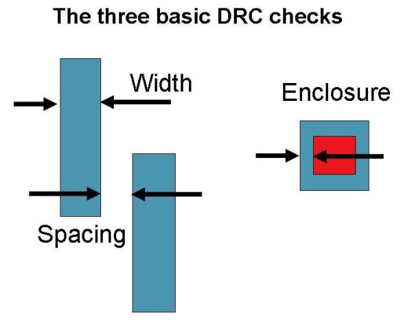
The 3D design tool must possess an array of features so that it can be of maximum use to the designers. One of the important features that must be present is 3D functionality that is design rule checker. This one is indeed one of the crucial features as the rules can be taken as a guide for the designers. The designers can take their designs to a whole new level with the help of 3D functionality and they are realizing it at a fast pace. In this world of fierce competition it is nothing but necessary to evolve with them so that you remain in the game.